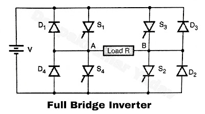
Full Bridge Inverter
Circuit Diagram of Full Bridge Inverter :
- The basic circuit for the single phase full bridge without the commutating components is as shown in Figure.
- Here it is assumed that the commutation is ideal and needs a very short times as compared to the total time of the output voltage waveform.
- The SCRS are turned on in pairs. First S1S2 conduct simultaneously and then S3 S4 conduct. With purely resistive load, the alternate firing of the thyristors S1S2 and S3 S4 will connect the dc source get connected across the load giving square wave output.
- The load current is in phase with the load voltage.
- The diodes D1 to D4, are known as the feedback diode they provide path for the load reactive energy now back to the head These diodes are inactive for a resistive load.
